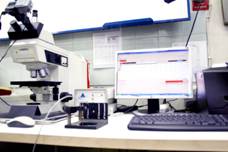
Metallographic optical microscope (Leica DMRX)
For optical imaging on the macro-scale, a metallographic optical microscope (Leica DMRX), equipped with digital cameras is used. The microscope can be used in polarized and phase contrast modes and can be combined with a thin-film-thickness measuring spectroscopic reflectrometer, through a c-mount adapter in a simple configuration (see below).
Thin-Film-Measurement Spectroscopic Reflectometer (NanoCalc 2000)
The system enables thickness measurements from 10 nm up to 250 μm (400 μm) for a large number of materials (semiconductors, polymers, glasses, resists, metals, oxides etc) by analyzing white light interference This is a non-destructive technique and does not need any special sample preparation. Up to three layers can be analyzed in the film stack. It can be combined with the Leica DMRX optical microscope.
The Leica DMRX optical microscope (left) combined with the Thin-Film-Measurement Spectroscopic Reflectometer (center).
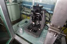
Macro-lensing imaging system
The macro-lensing-imaging system is equipped with CCD cameras for surface imaging at long working distances with micrometric resolution. The system allows for real time photonic surface processing.
Atomic Force Microscope (Quesant, Q-ScopeT 250)
The Atomic Force Microscope is equipped with a 40-μm Dual PZT scanner. The available scanning modes are Contact AFM-Z Height and Lateral Force, Intermittent Contact AFM (WaveModea) and Phase Mode. Besides AFM, Magnetic Force Microscopy option is available.
The Q-ScopeT 250 is operating inside an acoustic and thermal isolation chamber and the stability of the system is controlled with a laser interferometer. AFM gallery (LINK already on website).
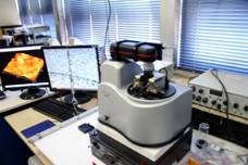
Scanning Probe Microscopy (Veeco di-Innova)
The Veeco di-Innova Scanning Probe Microscopy (SPM) provides high resolution scanning, and wide range of functionality for physical chemistry and materials science. It offers a fully complement of SPM techniques providing surface characterization of sample both in air and liquid, such as:
Contact Mode; Tapping Mode; Later Force Microscopy (LFM); Scanning Tunneling Microscopy (STM); Magnetic Force Microscopy (MFM); Phase Imaging; Conductive Atomic Force Microscopy (C-AFM); Scanning Thermal Microscopy (SThM); Force Distance Spectroscopy.
A closed-loop scanner (100 x100 μm2 and Z > 7.5 μm) or an open-loop scanner (5 x 5 μm2 and Z > 1.5 μm) are available.
The di-Innova system is placed on a vibration isolation table (K-Minus Technology).
Processing of materials at the nano-scale.
The Veeco di-Innova Scanning Probe Microscopy (SPM) besides bearing unique imaging and analytical capabilities at the nano-scale, can operate as a nano-lithographic tool with 1 nm resolution. In addition sub nano-meter resolution etching can be achieved in the Z direction with the VUV micro-maching apparatus.